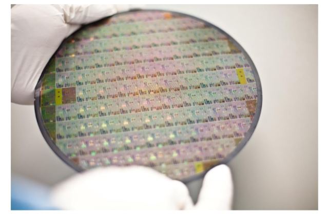
The Southampton Nanofabrication Centre has an extensive range of dry etch systems and wet etching competences for various research interests in silicon processing, metal etching, dielectric machining, thin film processing and other semiconductor materials (Type II, III, V, and N). High resolution pattern transfer features from micron to nanoscale is done through reactive gas chemistry and plasma etch technology. Wet etching provides a simple and cheap method of pattern transfer after lithography.
Deep Reactive Ion Etching (DRIE)
This system utilises the Advanced Silicon Etch (ASE) Technology, based on the Bosch process, to achieve rapid and very deep silicon etch profile with smooth sidewall. Our tool can characteristically accommodate from sized sample to 200 mm wafers. The sidewall angle accuracy is 90±1° with the roughness down to 20nm. This etching process is particularly suitable for silicon-based MEMS and NEMS devices where anisotropic profiles are essential. Can process Si based materials (Si, poly Si, Si3N4, SiGe) and III-V materials (InGaAs, InP).
- Deep Si etcher
- Can accommodate smaller samples up to 200mm wafer.
- SF6/C4F8/Ar/O2 gases
- Etch rates typically of >2um/min at 5um, >7um/min at 80um
- 90+1°, 20nm rms sidewall roughness,
- Aspect ratio - PR>30:1, SiO2>60:1
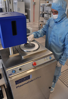
Reactive Ion Etching
The etch mechanism of RIE is achieved by using the reactive gas plasma generated by strong RF source to chemically ion etch the material of the samples. Depending on the process recipe, the material's etched profile can achieve high anisotropy. Typical gases available are CHF3, Ar, CF3, O2. In addition to substrate etching the RIE systems can also be used for clearing resists or other contaminants off the substrates. We house three Plasmalab systems that are distinguished by the available gases and metal/metal-free substrates processing
Plasmalab 80 plus (I) – Two Fluorine-based chemistry etching tools, alternatively argon and oxygen. Ideal for silicon (amorphous, poly), silica, silicon nitride, polymer, metal and resist residue cleaning. One tool is dedicated for non-metal containing substrates etching.
Plasmalab 80 plus (II)- Chlorine-based chemistry etching. Ideal for metal etching and suitable for III-V semiconductor materials.
- Gases available: CHF3, Ar, CF3, O2
- SiO2 etch: CHF3/Ar, >30nm/min, PR>3:1, SiN>2:1, Si>5:1
- Si3N4 etch: CHF3/O2/CF4, >50nm/min, >80°, PR>1.5:1, SiO>2.5:1, Si>5:1.
- PR de-scum: O2 >100nm/min
Inductively Coupled Plasma Etching (ICP)
The etching plasma is created by an RIE RF source and RF induction magnetic coil to produce high plasma densities. The results are high etch rate, high aspect ratio, and anisotropic etching of material of the samples. In addition, the systems can operate in ICP or RIE mode separately. We have two ICP systems dedicated for metal-contaminated and metal-free processes
- Plasmalab System 100 – Dielectric and Si Etcher
- Fluorine-based chemistry etching. Ideal for deep oxide etching, BPSG, TEOS, rare earth oxide, poly-silicon, polymer and diamond based material.
- SiO2 Etch: C4F8/O2, >200nm/min, PR>1:1
- PolySi aniso etch: SF6/O2, >300nm/min, PR>3:1, SiO3>7:1.
- PolySi iso etch: SF6, >1um/min, PR>50:1, SiO2>100:1
- Polymer etch: O2/N2, >300nm/min, PR 1:1, SiO2>10:1
- Plasmalab System 100 – Metal, Dielectrics and Si Etcher
- Chlorine/bromine-based chemistry etching. Ideal for metal etching, poly-silicon gate, platinum, III-V and III-N based semiconductor materials.
- Al etch: Cl2/HBr, >150nm/min, PR>2:1, SiO2>5:1
- PolySi gate etch: Cl2/HBr/O2, >100nm/min, PR>2:1, SiO2>100:1
- Au, Cr, Si, InP and Pt etch chemistries available
Ion Beam Etching (IBE)
Working on the similar principle as the reactive ion etcher but is assisted by an energised ion beam for the etching mechanism. This can achieve very high aspect ratio profiles, high etch rate and uniformity over a large sample. The system can handle up to 200 mm diameter wafer and sample can be tilted to perform angular etch. We have an Ionfab 300 plus that is configured for MEMS and NEMS structures, silicon-based material, silica, quartz and deep etch structures.
- Reactive ion beam etcher
- Can take up to 200 mm wafers
- Substrates can be tilted to perform angular etch
- Capability to etch significant range of materials including but not limited to Si, Ge, GaN, sapphire and metals
- Surface Decontamination Systems
- UV Ozone Cleaner:Used for remove surface contaminants, UV curing, improve surface hydrophobicity, oxidise surface of substrates.
- Oxygen Plasma Etching Systems:We have two Oxygen plasma ashing systems for stripping resists and de-scumming substrates. Can process up to 25 wafers of up to 200 mm wafers size in one batch.
- Wet Etching and Cleaning
| Wet Etch | Comments |
|---|---|
| 7:1 buffered hydrofluoric acid | Thermal oxide etch, rate 100nm/min |
| 20:1 buffered hydrofluoric acid | Thermal oxide etch, rate 100nm/min |
| Orthophosphoric acid @ 160C | Silicon nitride etch, rate 160nm/hr |
| Orthophosphoric acid @ 37°C | Aluminium etch, rate 0.1um/min |
| Potassium hydroxide @ 70°C | Silicon anisotropic etch, rate 0.7um/min |
| RCA clean | Wafer clean |
| Fuming nitric acid | Resist strip and wafer clean |